
News and events
A mailing list for magic mirror related discussions was created.
The 6th Makyoh Conversazione, the first international one in the series, successfully took place in Kindi University, Osaka, Japan on August 29–31, 2025. See the events website for program, abstracts and further information.
Introduction and basic principles
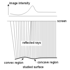
The assessment of the flatness and surface morphology of substrates is essential in modern semiconductor technology. This refers not only to the assessment of the incoming wafers but to the process monitoring as well, since several technological steps (metallization, epitaxy, layer deposition, patterning) may change the flatness of the sample. Several optical methods are in use for flatness assessment, e.g. laser interferometry or the Newton ring method. A less known but powerful optical method is the so-called Makyoh topography (Makyoh is a Japanese word, meaning ‘magic mirror’ and refers to an ancient mirror of sacred use: the mirror reflects the relief pattern engraved on its back to a distant wall). The principle of the method—as well as the explanation of the magic property of the ancient mirror—is the following: The mirror-like surface under test is illuminated by a parallel light beam, and the reflected beam is intersected by a screen. If the surface is perfectly flat, a uniform light spot appears on the screen. If the surface possesses deviations from the flatness, these deviations disturb the homogeneity of the reflected beam, and an image that is related somehow to the surface morphology appears on the screen (see figure on the left). The main advantages of the method, as compared to other optical methods, are its simplicity, inexpensiveness, real-time operation and high sensitivity.
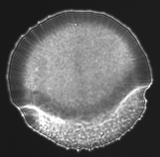
The image on the right shows the Makyoh topograph of a Si wafer. The image shows contrast variations on different scales corresponding to the surface morphology. In addition, diffraction features can be seen near the wafer edges.
Makyoh can be made quantitative by inserting a square grid into the path of the illuminating beam. The distortion of the grid image is related to the surface topography: the displacement of the grid node positions as compared to those obtained using a flat reference mirror, is proportional to the the surface gradient. The topography can be calculated by integrating the gradients.
Research and activities at MFA
The research on Makyoh topography commenced at the legal predecessor of MFA in the beginning of 1990s, after the first major wave of publications. It was continued at MFA with renewed intensity starting in 1998 . Our main results are as follows:
- geometrical optical model of the image formation
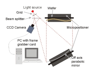
- construction of a unique, mirror-based system virtually free from optical aberrations and parallax errors (see figure below) and a set-up based on two spherical mirrors suitable to cost-efficient scaling-up for large-diameter samples
- developing algorithms for the grid-based evaluation of the topography
- exploring the possibilities beyond semiconductor wafers: studying the deformation of MEMS structures, the morphology of polished cross sections of renal stones and various non-semiconductors bulk and layered materials
- exploring the aspects of the image formation related to the ancient mirror
- representation in popular science
Makyoh topography is now routinely applied in our laboratory for the qualitative and quantitative assessment of semiconductor wafers and other mirror-like surfaces in-house as well as in various collaboration projects. Our equipment is capable to study wafers with diameter up to 5″. The largest measurable curvature radius is about 300 m; this corresponds to about 10 µm bowing projected to 5″ diameter.
Main publications
- F. Riesz, Geometrical optical model of the image formation in Makyoh (magic-mirror) topography, J. Phys. D: Appl. Phys. 33, 3033-3040, 2000.
- I. E. Lukács, Zs. Vízváry, P. Fürjes, F. Riesz, Cs. Dücsõ and I. Bársony, Determination of deformation induced by thin film residual stress in structures of millimetre size, Adv. Eng. Mater. 4, 625-627, 2002.
- I. E. Lukács, F. Riesz and Z. J. Laczik, High spatial resolution Makyoh topography using shifted grid illumination, Phys. Stat. Sol. A 195, 271-276, 2003.
- I. E. Lukács and F. Riesz, Makyoh-topography assessment of etch and polish removal of processed circuits for substrate re-use, Microel. Engin. 65, 380-386, 2003.
- F. Riesz, Makyoh-topography assessment of the deformation of micromachined membrane structures on double-side coated substrates, Sensors Actuators A 102, 123-129, 2002.
- F. Riesz, L. D. Pramatarova, R. Pramatarova and A. L. Tóth, Makyoh-topography studies of the morphology of the cross sections of renal stones, J. Crystal Growth 245, 101-108, 2002.
- F. Riesz, Makyoh topography: a simple yet powerful optical method for flatness and defect characterisation of mirror-like surfaces, Proc. SPIE 5458, 86-100, 2004.
- F. Riesz, Non-linearity and related features of Makyoh (magic-mirror) imaging, J. Optics 15, 5709, 2011.
- F. Riesz, Structured-illumination Makyoh-topography: optimum grid position and its constraints, Surface Topography: Metrology and Properties 6, 045009, 2018.
- F. Riesz, Modelling of the backside pattern transfer in magic mirror (Makyoh) imaging, J. Optics 25, 025602, 2023.
- F. Riesz, Visual approach to the imaging of magic mirrors (Makyohs), Results in Optics 12, 100477 , 2023.
Project participation
- Experimental and theoretical studies of the image formation mechanism of Makyoh topography (national – OTKA F 25224, 1998–2000)
- Micromachined Circuits for Microwave and Millimeter Wave Applications – MEMSWAVE (INCO–COPERNICUS No. 977131, 1998–2001)
- Quantitative Makyoh topography (national – OTKA T 037711, 2002-2006)
- Flexibile Makyoh topography (national – GVOP, 2006)
- Contract for building a Makyoh topography set-up at Fraunhofer Institute in Erlangen (2006)
- Hybrid Substrates for Competitive High Frequency Electronics – HYPHEN (from 2005 October to 2009 April)
- European Integrated Activity of Excellence and Networking for Nano and Micro-Electronics Analysis – ANNA (from 2006 December to 2010 November)
- Materials for Robust Gallium Nitride (MORGaN, from 2008 November to 2011 October)
- Novel methods for the flatness characterisation of mirror-like surfaces (semiconductor wafers) (national – OTKA K 68534, from 2007 July to 2011 June)
- Development of components for new-generation neutron instrumentation (Új generációs neutronos vizsgálóberendezések komponenseinek fejlesztése, national – KMR_12-1-2012-0226, from 2012 November to 2015 April)
- Mobility projects with the University of Oxford, Fraunhofer Institute in Erlangen, Institute of Materials for Electronics and Magnetism (IMEM-CNR, Parma, Italy) the Institute of Physics of the Polish Academy of Sciences and the Institute of Solid State Physics of the Bulgarian Academy of Sciences
Contact
Ferenc Riesz, riesz.ferenc@ek.hun-ren.hu
Past participants
János P. Makai
István E. Lukács
István Réti
Imre Eördögh
Béla Szentpáli